AI inference hits memory Wall, sparking hardware shakeup
The gist
AI inference has smashed headlong into the 'memory wall,' forcing a radical rethinking of hardware, software, and data center design to keep up with ever-hungrier large language models.
What to know
- By 2026, GPUs like NVIDIA's H100 are left twiddling their silicon thumbs—using just 1% of their compute during decoding—thanks to the transformer KV cache's quadratic memory demands.
- SRAM-centric chiplets like d-Matrix’s Corsair (150 TB/s bandwidth) and hybrid memory stacks are slashing bottlenecks, while new rack-scale systems like NVIDIA’s Vera Rubin shift the focus from raw FLOPS to tokens-per-megawatt.
- Two-thirds of recent efficiency gains come from clever software tricks—think KV cache compression and multi-token speculative decoding—outpacing even the fastest hardware upgrades.
Memory Bottleneck Redefines AI
AI inference is now throttled by memory bandwidth and KV cache growth, leaving GPUs idling and forcing a shift from compute-centric metrics to memory-first engineering.
By early 2026, the AI community had crystallized the understanding that memory bandwidth and capacity, rather than raw compute power, are the primary bottlenecks in large language model (LLM) inference—especially during the decode phase. Roofline model analyses revealed that decode workloads operate at an arithmetic intensity of merely 1 to 4 FLOPs per byte, dramatically below the compute-to-bandwidth ratio of leading GPUs like NVIDIA's H100, which requires around 295 FLOPs per byte to fully utilize its compute units. This mismatch means GPUs run at roughly 1% of their theoretical peak during decoding, leaving 99% of compute silicon idle while waiting on memory transfers, a phenomenon succinctly captured by the analogy that inference performance is limited by 'the door' (memory bandwidth) rather than 'the chefs' (compute units).
The structural cause of this memory bottleneck lies in the transformer architecture's quadratic scaling of self-attention and the ever-growing key-value (KV) cache during inference. As models generate tokens sequentially, each new token requires reading the entire KV cache from high-bandwidth memory, imposing a 'quadratic tax' that severely strains memory bandwidth and capacity. This challenge is compounded by the linear growth of the KV cache with context length, creating a 'brutal, non-negotiable reality' where increasing context or user concurrency inflates memory demands beyond what current hardware can efficiently handle, limiting batching and economic efficiency.
Industry leaders like NVIDIA have acknowledged this paradigm shift, with CEO Jensen Huang emphasizing that token generation is fundamentally bandwidth-constrained, not compute-constrained. To address these limits, NVIDIA developed the Grace Blackwell NVLink72, a rack-scale system integrating 72 chips to pool memory bandwidth and overcome single-chip bottlenecks, achieving a 50x performance gain in just two years. This strategic pivot away from chasing raw FLOPS toward optimizing data movement underscores a broader realization: optimizing for traditional compute metrics like model FLOPS utilization (MFU) can be misleading, and engineering efforts must focus on alleviating memory bandwidth and capacity constraints to unlock real inference throughput improvements.
This recognition has spurred a fundamental shift in AI hardware design philosophy, as exemplified by companies like Rebellions AI, which prioritize balanced compute-memory architectures over raw compute power. Their second-generation processors integrate large on-chip SRAM with HBM3 high-bandwidth memory in a memory-centric design that maximizes bandwidth and energy efficiency, delivering superior cost and power performance for inference workloads compared to traditional GPUs. As CEO Sunghyun Park notes, this memory-driven approach redefines the performance equation by focusing on maximizing tokens per second while minimizing power and cost, reflecting the industry's move to embrace memory as the new frontier in AI inference optimization.





SRAM & Hybrid Memory Revolution
SRAM-powered chiplets and hybrid memory stacks like HBF are breaking bandwidth barriers, but scaling up capacity demands radical integration and new packaging breakthroughs.
The emergence of SRAM-centric digital in-memory compute (DIMC) architectures marks a pivotal shift in AI inference hardware by tightly integrating high-bandwidth SRAM directly with compute cores to drastically reduce the memory bottleneck. d-Matrix’s Corsair chiplets exemplify this innovation with 256 DIMC cores and 256 MB of SRAM delivering up to 150 TB/s bandwidth—orders of magnitude beyond traditional HBM’s 2 TB/s—enabling inference workloads up to 10 times faster and five times more energy-efficient than GPUs. However, SRAM’s inherently low density limits capacity, necessitating multi-chiplet scaling strategies to handle large models, as a single chiplet’s 256 MB SRAM falls short of the 65 GB required for a 120 billion parameter GPT model.
To address SRAM’s capacity constraints, industry leaders are innovating hybrid memory architectures that blend SRAM’s ultra-low latency with emerging high-capacity memories like High-Bandwidth Flash (HBF). Companies such as SK Hynix and Micron are pioneering the 'H³' approach, combining HBM and HBF to balance bandwidth and capacity for specialized inference workloads. Google’s TPU architecture leverages this heterogeneity by storing static weights and KV caches in HBF while reserving HBM for dynamic data, significantly boosting large-scale approximate nearest neighbor search performance. Yet, the heterogeneous 3D stacking of NAND, SRAM, and logic chips in HBF introduces complex packaging and yield challenges, contributing to NVIDIA’s cautious stance on HBF adoption despite its massive 4TB capacity potential.
The SRAM-centric paradigm has inspired wafer-scale integration efforts to overcome capacity limits by creating massive monolithic chips packed with SRAM, such as Cerebras Systems’ WSE-3, which integrates 44GB of on-chip SRAM and nearly one million AI compute cores on a single wafer. This approach trades off memory capacity per chip against latency and energy efficiency, requiring hundreds of interconnected chips to serve trillion-parameter models but delivering deterministic execution with zero cache misses, as seen in Groq’s Language Processing Unit (LPU) architecture. This evolution from general-purpose CPUs to highly specialized LPUs underscores a strategic focus on minimizing off-chip memory movement to accelerate latency-sensitive AI inference workloads.





Disaggregated Hardware Takes Over
Inference is splitting into specialized hardware for prefill and decode, as industry giants abandon one-size-fits-all GPUs in favor of phase-optimized, multi-silicon systems.
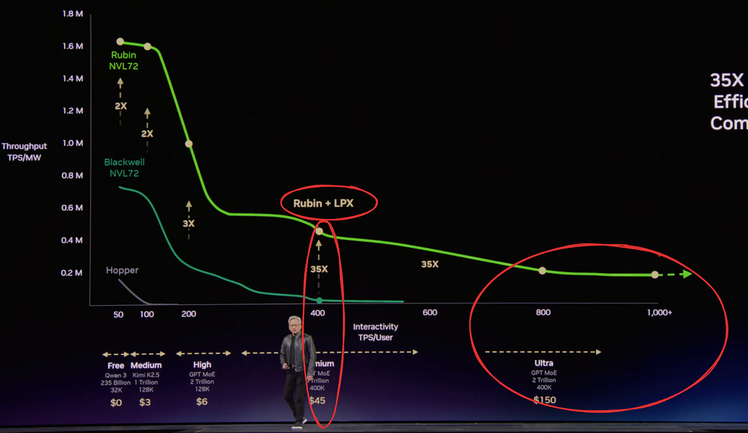
By early 2026, the AI industry had decisively embraced disaggregated inference architectures, moving beyond the GPU-centric paradigm to heterogeneous systems that split workloads into prefill and decode phases. Nvidia, while maintaining its vertical integration strategy with Rubin GPUs paired with Groq LPUs to optimize latency and throughput trade-offs, acknowledged that no single hardware suits all inference tasks equally. This multi-silicon approach reflects a recognition that hardware optimized for high-throughput batch processing is ill-suited for latency-sensitive token generation, necessitating specialized accelerators for distinct workload phases.
The March 2026 collaboration between AWS and Cerebras crystallized this architectural evolution by explicitly splitting AI inference into prefill and decode phases handled by distinct hardware: AWS Trainium chips for compute-heavy prefill and Cerebras wafer-scale engines for memory-bandwidth-intensive decode. This design leverages the opposing resource demands of each phase—prefill’s low memory bandwidth but high compute intensity versus decode’s high memory bandwidth and latency sensitivity—thereby avoiding the compromises inherent in single-GPU solutions and promising several-fold performance gains within Amazon Bedrock’s inference tiers.
Following AWS and Cerebras, AMD partnered with Cerebras to deploy a disaggregated inference infrastructure combining AMD Helios GPU racks for prefill and Cerebras wafer-scale engines, boasting 44 GB/s memory bandwidth—approximately 2,000 times that of Nvidia GPUs—for decode. This collaboration aims to deliver the fastest, highest-throughput, ultra-low latency AI inference system, exemplifying the broader industry trend toward decoupling memory and compute resources to overcome bottlenecks and optimize cost and performance at scale.
This shift toward disaggregated and specialized inference architectures marks a new era of silicon specialization and systems-level competition in AI hardware. Major players like Nvidia, AMD, Intel, and AWS are orchestrating heterogeneous hardware stacks—pairing GPUs, LPUs, wafer-scale engines, and AI ASICs—to address the divergent physics of prefill and decode workloads as AI moves from demos to production scale. As one analysis put it, inference has become a 'systems business' where owning the full stack, not just a chip, is essential to achieving superior utilization, cost efficiency, and latency, heralding a fundamental transformation in datacenter design and vendor strategy.


Rack-Scale AI Factories Arrive
NVIDIA’s Vera Rubin racks unify compute, memory, and networking into modular, liquid-cooled AI factories—locking in customers and transforming data center economics.
By early 2026, NVIDIA pioneered the development of rack-scale integrated AI inference systems with its Rubin and Vera Rubin platforms, which unify six critical silicon domains—compute, memory, communications, storage, power, and networking—into a cohesive rack-scale AI factory unit. The Vera Rubin NVL72 rack, featuring 72 Rubin GPUs and 36 Vera CPUs interconnected via NVLink 6, achieves unprecedented intra-rack bandwidths of 260 TB/s and coherent CPU-GPU interconnects at 1.8 TB/s, enabling tightly coupled heterogeneous computing that transcends traditional standalone GPU deployments. This system-level co-design, exemplified by innovations like the Superchip packaging two Rubin GPUs and one Vera CPU on a single board, marks a strategic shift from component sales to delivering turnkey, template-based racks that redefine AI data center infrastructure.
NVIDIA’s embrace of disaggregation and heterogeneous integration extends beyond GPUs and CPUs to include DPUs, networking, and storage components, such as BlueField-4 DPUs and ConnectX-9 SuperNICs, which actively participate in the AI inference pipeline by accelerating KV cache data and reducing cross-host traffic. This holistic approach addresses critical memory bottlenecks and latency challenges inherent in large-context and agentic AI workloads, as evidenced by the Vera Rubin platform’s ability to support always-on inference with very long token contexts. The resulting rack-scale systems not only optimize raw performance but also dramatically improve power efficiency, with Vera Rubin reportedly generating ten times more tokens per second per megawatt than its predecessors.
NVIDIA’s vertical integration strategy for rack-scale AI systems aims to lock in customers by bundling silicon, networking, software, and mechanical design into modular, cable-less racks that demand redesigned power delivery and liquid cooling infrastructures capable of handling 220 kW-class densities. This approach not only raises switching costs but also leverages NVIDIA’s control over supply chains and system specifications to establish dominance in the AI infrastructure market. Early deployments by hyperscalers and AI infrastructure providers like CoreWeave and Nebius validate this model, with production scaling globally across over 350 factory sites and major cloud platforms, signaling NVIDIA’s evolution from a GPU vendor to a comprehensive AI platform integrator.
The Vera Rubin platform epitomizes a paradigm shift in AI infrastructure economics, moving away from raw GPU TFLOPS as the primary metric toward system-level efficiency measured by tokens generated per megawatt of power. Architectural innovations distribute performance demands across advanced packaging, HBM4 memory, high-bandwidth NVLink fabrics, and sophisticated power and cooling systems, enabling up to a 90% reduction in inference cost per token compared to previous generations. This evolution underscores the critical importance of rack- and pod-level integration and bandwidth in sustaining the next generation of AI workloads, where holistic design and multi-supplier collaboration are essential to overcoming the AI memory bottleneck at scale.


Software Outpaces Silicon Gains
Software-driven advances in KV cache compression, quantization, and decoding have delivered bigger inference efficiency leaps than new hardware, slashing costs and boosting throughput.
By early 2026, a wave of architectural and software innovations converged to tackle the AI inference memory bottleneck, focusing on reducing the bytes of KV cache per token and the volume of model weights loaded per decode step. Techniques such as GQA, hybrid attention/SSM, sliding window, and MoE architectures directly targeted these metrics, recognizing that inference speed and cost hinge more on memory bandwidth than raw FLOPs. Companies like DeepSeek exemplified this trend by co-designing algorithms alongside custom storage layers to optimize data flow, echoing Jensen Huang's emphasis on mastering the memory subsystem to keep GPUs fully utilized.
Throughout 2024 and 2025, software and model-side improvements outpaced hardware gains in driving AI inference efficiency, accounting for roughly two-thirds of the progress. Industry leaders such as Anthropic, Google, and DeepSeek deployed sophisticated KV cache compression, reuse, and management strategies that dramatically lowered token serving costs and enabled providers to reduce input token prices. NVIDIA's own benchmarks underscored this impact, showing a 1.5× throughput boost on the same H100 hardware for Llama 2 70B purely from software updates, while open-source enhancements like multi-token speculative decoding nearly doubled throughput on consumer GPUs without any hardware changes.
Recent breakthroughs in KV cache quantization and attention mechanisms have further compressed memory footprints and accelerated decoding speeds without sacrificing accuracy. The OScaR framework, introduced in mid-2026, innovatively addressed Token Norm Imbalance to enable near-lossless INT2 quantization, achieving up to 5.3× memory reduction and 4.1× throughput gains over previous BF16 baselines. Complementing this, production-grade FP8 quantization and kernel-level optimizations like NVIDIA's NVFP4 format and FlashAttention kernels have slashed memory bandwidth demands and boosted arithmetic throughput, collectively enabling up to 5× end-to-end inference speedups on modern GPUs.
Beyond raw compression, software innovations have refined AI inference workflows and decoding strategies to maximize efficiency and fidelity. Techniques such as multi-step delegation pipelines, as demonstrated by Microsoft Research, maintain output quality with under 1% degradation over many iterations, while speculative decoding methods like EAGLE-3 leverage small draft models to propose multiple tokens, verified in parallel by larger models, achieving 2–4× faster decoding with mathematically identical outputs. These advances, alongside architectural shifts reducing memory per token, are critical as agentic workloads surge token consumption, pushing providers to optimize memory bandwidth aggressively amid hardware bandwidth ceilings on GPUs like Nvidia's H100 and A100.






AI Hardware Goes Multi-Model
Startups and hyperscalers are abandoning monolithic GPUs for diverse, workload-specific chips and memory fabrics, splintering the market into a competitive multi-silicon landscape.
By mid-2026, the AI hardware ecosystem has rapidly diversified beyond traditional GPU-centric designs, with startups like NextSilicon and Majestic Labs pioneering fundamentally different architectures that replace GPUs with novel memory hierarchies and processor designs. NextSilicon targets HPC workloads with a radically new inference architecture that addresses the critical memory bottleneck, aiming for up to 1,000× efficiency improvements over GPUs, while Majestic Labs leverages custom Arm-powered AI processing units paired with up to 128TB of unified LPDDR6 memory, vastly expanding memory capacity and reducing costs by 10 to 50 times compared to equivalent GPU systems. This evolution underscores a shift from incremental transistor scaling to architectural innovation focused on balancing compute and memory to overcome energy inefficiencies inherent in current designs.
The emergence of hybrid and disaggregated memory fabrics is reshaping AI hardware infrastructure, as exemplified by SK Hynix’s H³ architecture combining HBM and High-Bandwidth Flash (HBF), and GenStorAIGE’s AI90 platform integrating PCIe Gen5 SSDs with HBM and system DRAM to extend memory capacity beyond traditional limits. Cloud giants like Google are leading the charge by embedding novel memory hierarchies into custom ASICs, optimizing data placement between static weights in HBF and dynamic data in HBM, while advanced packaging techniques such as 3D stacking with TSV and hybrid bonding enable tighter integration of heterogeneous memory types. This trend points to a future where AI systems are tailored with workload-specific memory architectures to maximize bandwidth and energy efficiency.
The AI hardware landscape is increasingly fragmented and specialized, with hyperscalers like Google investing tens of billions annually in diverse ASIC programs and startups such as Groq, Cerebras, Maia, MTIA, and Trainium pursuing unconventional architectures that break the mold of the standard compute-plus-HBM design. This proliferation of heterogeneous chips reflects recognition that current architectures often represent local minima in optimization, prompting multiple parallel design efforts even within single organizations to avoid lock-in. As AI workloads disaggregate into training, cloud and edge inference, and agentic processing, the market is evolving into a multi-silicon, multi-model environment where efficiency, memory architecture, software ecosystems, and deployment economics outweigh raw performance metrics.
Collaborative regional ecosystems and rack-scale innovations are shaping the future of AI hardware, as seen in Rebellions AI’s memory-centric processors combining large on-chip SRAM with HBM3 and their delivery of large-scale rack deployments exceeding one hundred racks worldwide. Strategic partnerships among semiconductor manufacturers, software firms, and telecom operators emphasize AI sovereignty by reducing dependence on single technology ecosystems and fostering diversified supply chains. Meanwhile, FuriosaAI’s development of servers with 16 PCIe accelerator slots and minimized fabric switches exemplifies the move toward specialized inference architectures with improved accelerator-to-switch ratios and adoption of advanced memory like HBM3E, underscoring a trend toward tightly integrated, workload-specific, and scalable AI infrastructure designed for the post-GPT era.