AI’s memory crunch: how bandwidth bottlenecks are rewiring the future of chips and data centers
The gist
Forget raw compute—AI's future is being bottlenecked by memory bandwidth, forcing a radical rethink of chips, data centers, and how the world powers artificial intelligence.
What to know
- By early 2026, top-tier GPUs like NVIDIA’s H100 were running at just 1% of their compute potential during AI inference, with memory bandwidth—not processing power—the real choke point.
- Breakthroughs like Ring Attention and aggressive quantization now let models handle millions of tokens and decode up to 3× faster by squeezing every byte of memory bandwidth.
- With up to 50% of CapEx flowing into memory infrastructure and even new power plants being built, the AI arms race is now a memory game—driven by tiered architectures and AI-powered software, not just bigger chips.
The Real GPU Bottleneck
AI inference workloads leave 99% of GPU compute idle as memory bandwidth, not processing power, emerges as the true limiter—forcing a rethink of hardware design and GPU origins.
By early 2026, the roofline model had crystallized the understanding that memory bandwidth, rather than compute capacity, is the fundamental bottleneck in AI workloads—especially during the decode phase of transformer models. For instance, NVIDIA's H100 GPU, despite its massive 989 TFLOPS FP16 compute capability, requires an arithmetic intensity of roughly 295 FLOPs per byte to fully utilize its compute units; yet decode workloads operate at a mere 1–4 FLOPs per byte, causing the chip to run at about 1% of its theoretical peak and leaving 99% of the compute silicon idle. This stark imbalance highlights a structural mismatch between what transformer decode demands and what current GPU architectures provide, a limitation that no amount of hardware scaling can fix.
While the decode phase is memory-bound, the prefill phase of transformers remains compute-bound due to its high arithmetic intensity—often exceeding 4,000 FLOPs per byte on FP16 precision—aligning well with GPU architectures optimized for massive parallelism. This duality underscores the critical importance of the compute-to-bandwidth ratio as the key metric for hardware sizing in large language model (LLM) workloads, where values above approximately 150 FLOPs per byte indicate compute-bound tasks and below 100 signal memory-bound performance. Consequently, hardware designs must balance these divergent demands, but the memory bottleneck during inference remains the more intractable challenge.
The origins of GPU memory in graphics rendering inadvertently laid the groundwork for modern AI scaling, as GPUs were initially designed with large memory capacities to handle textures, lighting, and physics in video games. This repurposing of vast memory resources has become foundational for holding enormous AI model parameters and context windows, with models like GPT-5.4 demanding upwards of 2 terabytes of VRAM to run on consumer hardware. Moreover, serious applications push context lengths to 256k tokens, further amplifying memory capacity and bandwidth requirements, which now eclipse raw computational power as the primary constraints in both training and inference.
In autoregressive LLMs, the sequential token generation process enforces strict dependencies that exacerbate memory bandwidth constraints, as each token’s computation requires streaming the entire model's weights—often over 140 GB—from high-bandwidth memory into the chip’s SRAM. This results in arithmetic intensities near 1 FLOP per byte, causing GPUs to operate at under 1% of their theoretical peak compute despite their blazing FLOPS. While software strategies like KV caches and batching frameworks help mitigate these limits by reducing recomputation and amortizing weight streaming, they introduce heavy memory residency costs and hit capacity ceilings as concurrency and context lengths grow. Consequently, hardware upgrades increasingly focus on expanding memory bandwidth and interconnect speeds—such as HBM4 and NVLink 5—rather than raw compute, though these remain economically challenging bottlenecks that define the future trajectory of AI infrastructure.




Software Rewrites the Rules
Breakthrough model architectures and memory-efficient algorithms like Ring Attention and FlashAttention are slashing memory needs per token, letting massive models run faster and cheaper without new hardware.
By early 2026, architectural innovations such as GQA, hybrid attention/SSM, sliding window mechanisms, and mixture of experts (MoE) models have converged on a common goal: drastically reducing the bytes of key-value (KV) cache per token and the bytes of weights loaded during each decode step. This focus stems from the realization that inference in large language models is primarily memory-bandwidth bound rather than compute-bound, with decode speed and cost dominated by memory transfers rather than floating-point operations. Consequently, strategies like aggressive quantization, fewer attention layers, and attention-less or linear alternatives directly cut latency and cost by minimizing the memory footprint per token, underscoring the critical role of software and model architecture in overcoming memory bottlenecks.
Innovative software techniques such as Ring Attention have reimagined distributed attention computation by partitioning input sequences across GPUs instead of model weights, enabling exact O(n²) global attention on ultra-long contexts—up to millions of tokens—that would otherwise require prohibitive memory per device. By overlapping communication and computation in a ring topology, Ring Attention effectively distributes the KV cache and mitigates network bandwidth bottlenecks, allowing models with 70B parameters to handle 1-million-token sequences without exceeding the memory limits of four H100 GPUs. This approach exemplifies how software-level architectural redesigns can circumvent hardware constraints to scale AI workloads.
Cutting-edge memory-efficient model serving techniques, exemplified by FlashAttention and the OScaR quantization framework, have further pushed the envelope by optimizing GPU memory usage and throughput. FlashAttention leverages ultra-fast on-chip memory to process attention computations in blocks, avoiding the need to materialize the full attention matrix and reducing memory transfer bottlenecks, achieving latency as low as 35 milliseconds. Meanwhile, OScaR introduces extreme KV cache quantization with near-lossless INT2 performance, delivering up to 3× decoding speedup and over 5× memory footprint reduction compared to BF16 baselines. These advances highlight how software and model architecture innovations—not just hardware—are pivotal in mitigating memory bottlenecks.
The relentless pressure of agentic AI workloads consuming millions of tokens per session has intensified the urgency for memory optimizations, as existing GPUs like the NVIDIA H100 and A100 hit decode throughput ceilings dictated by memory bandwidth rather than compute power. This bottleneck has shifted industry focus toward software and model-side innovations—such as activation checkpointing, CPU offloading of transformer inputs, and tiling computations across sequence length—that reduce memory usage per token and enable training and inference at unprecedented context lengths, sometimes reaching millions of tokens. As IBM and others emphasize, memory requirement has become the new currency in AI model performance, driving a wave of co-designed software-hardware solutions that keep GPUs efficiently utilized despite hardware constraints.



Memory as a Tiered Mountain
AI data centers now juggle a complex hierarchy of memory—from lightning-fast on-chip caches to emerging high-bandwidth flash—driving new strategies and hardware to manage cost, speed, and scale.
By early 2026, the GPU memory hierarchy was well understood as a tiered mountain of tradeoffs, where ultra-fast but tiny registers and caches sit atop larger but slower memory like HBM, host RAM, and network storage. This layered architecture, exemplified by NVIDIA's H100 GPUs with 2-3.35 TB/s HBM bandwidth tightly integrated via 3D chip stacking, imposes critical latency and bandwidth constraints that shape AI workload optimization strategies such as activation checkpointing and model parallelism. The fundamental tension remains that faster memory is always smaller and more expensive, forcing practitioners to carefully orchestrate data movement to mitigate costly transfers across these levels.
To alleviate memory bottlenecks, the industry has embraced hierarchical memory management combined with faster interconnects like PCIe Gen 5 and NVSwitch, enabling high-speed GPU-to-GPU communication at 900 GB/s within nodes, though inter-node links remain significantly slower. Techniques such as prefetching batches ahead and offloading data to CPU memory help overlap computation and data transfer, while pipelining and expert parallelism across multiple GPUs and racks further optimize memory usage and minimize idle time during large language model training. Hyperscalers reportedly allocate up to 50% of their CapEx to memory infrastructure, underscoring its centrality in scaling AI workloads.
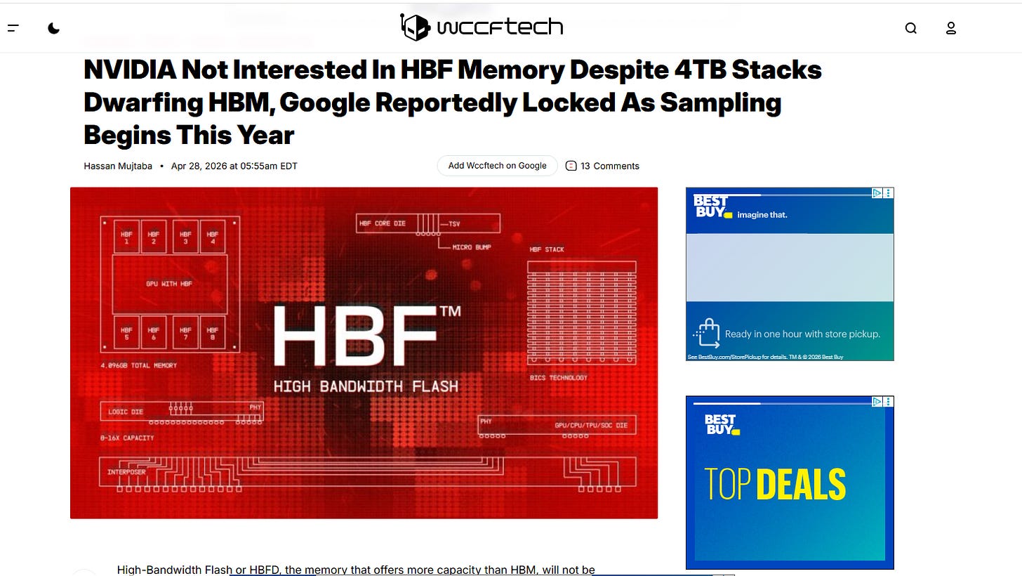
Emerging hardware innovations are challenging the traditional GPU-memory paradigm. Startups like NextSilicon are developing fundamentally different chip architectures that tightly integrate memory and compute to overcome the memory bandwidth bottleneck, promising up to 8× performance gains through novel techniques including memory compression. Meanwhile, high-bandwidth flash (HBF) memory, offering 10 to 16 times the capacity of HBM at a fraction of the cost, is gaining traction for AI inference workloads despite NVIDIA's current reluctance due to NAND flash’s limited write endurance and early manufacturing challenges. Industry leaders such as SK Hynix and Micron are pioneering hybrid memory architectures (H³) combining HBM and HBF to create tiered systems that better meet AI’s capacity, bandwidth, and cost demands.
By mid-2026, the shift toward tiered memory hierarchies tailored for AI workloads became evident with innovations like Apple's AFM 3 Core Advanced architecture, which stores entire 20-billion-parameter models in NAND flash and dynamically loads selected experts into DRAM per prompt. This approach circumvents traditional DRAM capacity limits by leveraging flash as persistent storage and employing prompt-level routing to manage bandwidth constraints. Complementing this, HBF technology, exemplified by Sandisk’s BiCS design, offers persistent, thermally stable, high-density memory optimized for AI inference at data centers and edge devices, marking a significant evolution toward hybrid memory systems that balance capacity, bandwidth, and energy efficiency.





AI Memory Goes Strategic
Memory infrastructure has become a national priority, with industry giants and governments reshaping standards, investing in power plants, and betting on AI-driven software to break through bandwidth barriers.
By early 2026, the AI infrastructure landscape witnessed a fundamental shift in memory strategy, with end customers like NVIDIA taking the reins in defining memory specifications based on real-world, large-scale deployments rather than traditional vendor-led standards. This evolution reflects a broader ecosystem transformation where nation-states also prioritize AI infrastructure, committing unprecedented sovereign resources such as new power plants to sustain datacenter expansion, underscoring memory bottlenecks as a strategic national and industrial challenge.
Amid soaring memory demands, industry players are pivoting from purely hardware-centric solutions to innovative AI-driven software optimizations. AMD’s 2026 acquisition of MEXT exemplifies this trend, leveraging AI-powered predictive memory tiering to effectively turn flash storage into DRAM-like performance, doubling to quadrupling usable memory capacity while slashing infrastructure costs by half. This strategic move not only enhances AMD’s data center portfolio but also signals a broader shift away from costly hardware stacking toward adaptable, software-driven memory management as the new frontier in overcoming memory bottlenecks.
Meanwhile, NVIDIA addresses AI inference memory bandwidth constraints through innovative resource pooling, exemplified by the Grace Blackwell NVLink72 rack-scale computer that integrates 72 chips to deliver a 50x performance boost within two years. CEO Jensen Huang highlights that the core obstacle is not chip scarcity but fragmented budgets and siloed institutional resources, advocating for centralized pooling to unlock AI infrastructure potential—a call echoed by academic institutions like Stanford, where isolated funding hampers shared compute capabilities critical for scaling AI workloads.
The memory ecosystem is also diversifying with hybrid architectures and tiered memory strategies gaining traction. While NVIDIA remains cautious about adopting High-Bandwidth Flash (HBF) due to technical and commercial hurdles, companies like Google have pioneered HBF adoption in custom TPU designs to optimize inference workloads, enabling massive on-chip vector databases. This momentum propels memory suppliers such as SK Hynix and Micron to develop hybrid HBM-HBF solutions, while advanced packaging technologies become essential enablers, creating new opportunities for chip design service providers and elevating NAND flash manufacturers like SanDisk into core AI infrastructure roles.