SK hynix bets big on AI memory with $720b expansion
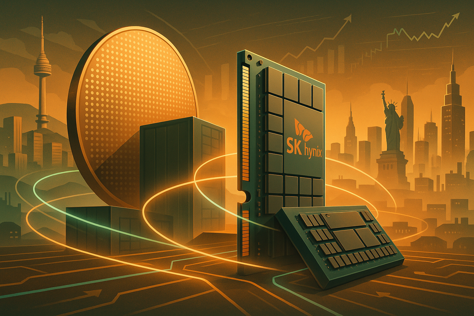
The gist
SK hynix is throwing down a colossal $720 billion bet to triple global AI memory capacity and cement its dominance in the high-stakes race for next-gen chips.
What to know
- SK hynix commands nearly 58% of the high-bandwidth memory (HBM) market and is expanding with exclusive deals—including Nvidia—amid surging AI demand.
- The company is breaking ground on a $3.87 billion advanced HBM packaging plant in Indiana, backed by up to $1.7 billion in U.S. government incentives and creating 7,000 jobs.
- Innovations like 20-high DRAM stacks and hybrid bonding tech are powering SK hynix’s leap in memory density, thermal performance, and strategic partnerships with Nvidia and Google.
AI Supercycle Fuels SK hynix Surge
SK hynix is tripling global HBM output and reshaping memory supply chains as its market cap soars past $1 trillion, driven by hyperscale AI demand and exclusive supplier status with Nvidia.
SK hynix is undertaking an unprecedented $720 billion investment to massively expand its global high-bandwidth memory (HBM) production capacity, a strategic bet on the explosive and sustained demand driven by AI technologies. This historic buildout aims to create the world’s largest network of memory factories, with plans to triple production capacity by 2034, reflecting the company’s confidence in AI’s transformative impact on memory consumption and supply dynamics.
Dominating the HBM market with a commanding share of approximately 57-58%, SK hynix has positioned itself as the critical supplier for AI chip leaders such as Nvidia, with whom it has secured exclusive long-term agreements. This leadership is underscored by the strategic reallocation of production lines from commodity DRAM to higher-margin HBM stacks, enabling SK hynix to capitalize on the AI-driven memory supply crunch and reinforce its market dominance amid constrained global supply.
The company’s market capitalization skyrocketed from $100 billion to over $1 trillion within sixteen months, a testament to investor confidence fueled by AI’s insatiable memory demands. SK hynix’s CEO Kwak Noh-jung warns that supply will remain tight well beyond 2030, with hyperscale cloud customers pre-committing $22 billion to secure HBM supply through 2027, highlighting the permanent reshaping of memory demand priorities in the AI supercycle.
SK hynix’s AI-driven expansion is supported by a global production footprint centered in South Korea, supplemented by facilities in China, Japan, and notably the United States, where it is breaking ground on an advanced HBM packaging plant in Indiana. This geographic diversification, combined with the company’s ability to self-fund through robust AI memory profitability and private equity interest, underscores SK hynix’s strategic commitment to scaling capacity and innovation to meet the evolving needs of AI workloads worldwide.

Next-Level Memory Stacking
Breakthroughs like 20-high DRAM stacks and hybrid bonding are setting new standards for memory density and thermal management, pushing HBM performance to meet AI’s relentless computing needs.
SK hynix is pushing the boundaries of HBM packaging by enabling unprecedented 16-high and 20-high DRAM stacks, tackling complex challenges such as die warpage, inter-die spacing reduction by about 50%, and enhanced thermal management. Their molded process, which bonds the entire DRAM stack in a single reflow and fills gaps with thermally conductive molding material, boosts productivity and thermal performance, albeit with increased sensitivity to die warpage that demands precise control.
Hybrid bonding emerges as a transformative packaging technology for SK hynix, allowing thicker silicon dies—up to 24% thicker within the same package height—and significantly improved thermal conductivity by roughly 35% at 20-high stacks. This innovation not only reduces bump spacing to less than 18 micrometers by eliminating microbumps but also supports stacking beyond 16 layers, addressing power and heat dissipation challenges critical for AI workloads.
To combat localized thermal hotspots in base dies, SK hynix is pioneering iHBM technology, embedding silicon heat blocks and high-thermal-conductivity, electrically insulating cooling components directly above hotspot regions. This targeted cooling approach reduces thermal resistance by over 30%, requiring early-stage co-optimization in design to integrate these solutions effectively rather than retrofitting them late in the product cycle.
SK hynix’s advanced packaging strategy extends beyond stacking height to encompass integrated solutions like Intel’s EMIB for next-generation HBM4, which boasts up to 24 Gb DRAM densities, 36 GB capacity, and 2048 GB/s bandwidth. This evolution towards 3D packaging structures, combined with tighter collaboration among memory companies, GPU designers, foundries, and packaging firms, reflects a holistic approach to overcoming mechanical stresses, interposer routing complexities, and the increasing demands of AI-driven memory architectures.
Strategic Alliances and IPO Ambitions
SK hynix is leveraging deep partnerships and pioneering tech standards to anchor the AI hardware ecosystem, while its anticipated U.S. IPO aims to dominate the HBM supply chain and lift the entire semiconductor sector.
SK hynix is cementing its role as a pivotal AI memory innovator through strategic collaborations with industry leaders like Nvidia, exemplified by the mass production of the 192GB ISOCAM M2 module tailored for Nvidia's Vera Rubin AI platform, which doubles conventional memory bandwidth. Complementing this, SK hynix and Sandisk’s launch of the High Bandwidth Flash (HBF) standard—developed alongside Google and Tenstorrent—leverages the open UCIe interconnect to enable seamless interoperability across diverse AI chip architectures, effectively bridging the gap between ultra-fast HBM and high-capacity SSDs and reducing reliance on proprietary ecosystems.
SK hynix’s pioneering advancements, such as the industry’s first 1C nanometer LPDDR6 memory offering a 33% speed boost and over 20% power efficiency gains, underscore its commitment to powering next-generation, real-time AI applications. This technological leadership has not gone unnoticed on Wall Street, where bullish analyst coverage from RBC Capital, Stifel, and William Blair highlights expectations of sustained AI-driven demand and anticipates favorable HBM contract repricing in 2027, positioning SK hynix as a key undervalued player in the AI hardware ecosystem.
The anticipated SK hynix IPO in the U.S. is more than a capital-raising event; it is a strategic maneuver to dominate the critical HBM supply chain that underpins AI processor performance. Beyond bolstering SK hynix’s market position, this move is poised to elevate valuations across the semiconductor manufacturing equipment sector, effectively lifting the entire AI hardware ecosystem by financing the infrastructure essential for sustaining the rapid growth of AI technologies, even as this speculative investment cycle introduces both opportunity and risk.


Indiana Plant Sparks U.S. Chip Hub
A $3.87 billion advanced packaging plant in Indiana—backed by massive public incentives and infrastructure upgrades—is turning the region into a semiconductor powerhouse and deepening SK hynix’s U.S. roots.
SK hynix’s groundbreaking of its $3.87 billion advanced packaging plant in West Lafayette, Indiana, marks a historic milestone as the largest single development project in the state and the company’s first U.S. high-bandwidth memory production base. Spanning 540,000 square meters—roughly the size of 75 soccer fields—the facility is projected to generate around 7,000 direct and indirect jobs across construction, R&D, and operations, while fostering close collaboration with Purdue University to recruit skilled engineers and deepen ties with local big-tech customers like Nvidia.
This ambitious expansion is underpinned by a robust partnership with U.S. federal, state, and local governments, which collectively provide SK hynix with up to $458 million in direct grants and $500 million in loans through the CHIPS and Science Act, complemented by Indiana’s commitment of $45 million for infrastructure and up to $712 million in tax incentives through 2055. Commerce Secretary Howard Lutnick has emphasized the strategic importance of such investments, stating a clear intent to attract Korean semiconductor giants like SK hynix to bolster domestic manufacturing and secure supply chains.
Supporting the plant’s operations involves extensive infrastructure upgrades, including a $20.3 million power supply project approved for Duke Energy Indiana, a 2.1-kilometer high-pressure gas pipeline by CEI North, and over $170 million invested by Air Liquide in industrial gas production facilities. Additionally, West Lafayette is expanding its wastewater treatment capacity from 10.5 to 15 million gallons per day, reflecting a comprehensive, multi-stakeholder approach to creating a state-of-the-art semiconductor manufacturing ecosystem.
SK hynix’s U.S. expansion strategy notably contrasts with its South Korean model by leveraging significant public and utility company investments to reduce upfront infrastructure costs, whereas in South Korea private firms typically shoulder about 70% of such expenses. This collaborative funding approach in Indiana not only lowers financial barriers but also exemplifies a strategic alignment between government incentives and industry needs to accelerate advanced semiconductor manufacturing capacity in the United States.