SK hynix, samsung race to redefine AI memory limits
The gist
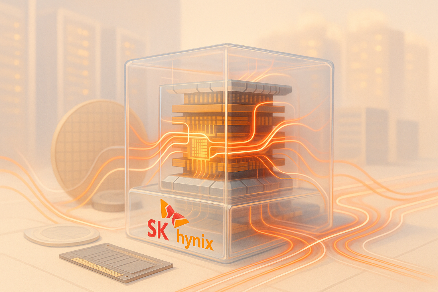
AI memory giants SK hynix and Samsung are smashing bandwidth and capacity barriers with optical interconnects, 3D stacking, and flash-powered architectures that could make today's HBM look quaint.
What to know
- SK hynix is integrating optics directly into AI memory packages, hitting over 100 Tbps per node with sub-10 ns latency to leap past HBM's bandwidth limits.
- Samsung's zHBM stacks DRAM atop accelerators, boosting bandwidth by 230% and power efficiency by 70%, while debuting compute-offload logic and advanced thermal management.
- High-bandwidth flash (HBF), co-developed by Sandisk, SK hynix, and partners, will deliver up to 16x HBM capacity with HBM-like speeds—and samples land later this year.
Optics Break the Bandwidth Wall
SK hynix’s co-packaged optics strategy transforms memory from a component into a system-level enabler, unleashing massive bandwidth and energy efficiency while redefining the AI data movement paradigm.
SK hynix is spearheading a transformative shift in AI memory architecture through its co-packaged optics (CPO) technology, which integrates optical interconnects directly within the same package as processors and memory. This optics-centric approach aims to shatter the traditional bandwidth ceiling imposed by HBM by delivering over 100 terabits per second per node with energy efficiency below 1 picojoule per bit and chip-to-chip latency under 10 nanoseconds. By replacing long copper electrical connections with optical links, SK hynix addresses the escalating 'bandwidth wall' caused by computing performance outpacing interconnect growth, enabling high-speed, low-latency data movement critical for scaling AI systems beyond current limits.
The company’s roadmap envisions a progressive evolution from 2D packaging to 2.5D photonic interposers and ultimately 3D heterogeneous integration, bringing optics ever closer to computing silicon. This strategy facilitates shared memory access across thousands of processors by directly connecting pools of XPUs and large memory arrays through high-bandwidth optical interposers, effectively enabling unified large-scale AI systems that transcend physical packaging constraints. Such integration not only enhances data transfer efficiency but also redefines memory suppliers like SK hynix as system-level partners designing AI infrastructure at rack and pod scales rather than mere component vendors.
SK hynix’s optics-centric architecture tackles fundamental physical and energy limitations inherent in copper-based interconnects, which suffer from signal loss and rising power consumption as speeds and distances increase. By minimizing the electrical signal travel distance within packages and leveraging optical engines for longer transmissions, the company enables scalable, energy-efficient AI infrastructure capable of supporting massive model training and data center demands. As Lee Kyu-sang emphasizes, 'Even if computing chips become more powerful, overall system performance cannot improve if data movement fails to keep pace,' underscoring optical transmission as the linchpin for future AI system scalability.
zHBM: Stacking Logic and Memory
Samsung’s zHBM fuses DRAM and accelerators into a single vertical stack, embedding compute offload and advanced thermal controls that make bandwidth—not raw capacity—the new AI performance frontier.
Samsung’s zHBM architecture revolutionizes AI memory integration by vertically stacking high-bandwidth memory directly atop AI accelerators, eliminating the traditional 2.5D interposer. This tight coupling not only boosts DRAM bandwidth by 230% compared to standard HBM4e stacks but also delivers a 70% improvement in power efficiency, significantly reducing I/O power consumption and silicon footprint. By minimizing data transfer distances, zHBM maximizes memory bandwidth—a critical factor for AI inference performance—as emphasized by Samsung’s US head Sangyeon Jo, who highlights that future AI success hinges more on bandwidth utilization than sheer memory capacity.
Samsung advances beyond conventional HBM designs by embedding sophisticated logic and compute offload capabilities into the base die of its custom HBM (cHBM), replacing the bulky PHY with a compact Die-to-Die interface. This transformation leverages advanced logic nodes like Samsung’s D1c and 4nm processes to reduce power consumption and active area, enabling the base die to act as an intelligent partner that offloads workloads from the accelerator. The roadmap envisions evolving from cHBM to Advanced HBM (AHBM) and ultimately to zHBM, integrating memory controllers and partial compute elements to expand capacity and reduce bandwidth demands—addressing AI’s growing need for massive KV caches and larger context windows.
Thermal management, a critical challenge in densely integrated 3D stacked memory, is tackled by Samsung’s innovative Heat Path Block (HPB) technology, which covers half of the PHY area and reduces peak temperatures by over 35%. This breakthrough enables safe embedding of complex logic such as memory controllers and SRAM-based cell repair within the base die without compromising power efficiency or system reliability. Complementing HPB, Samsung applies advanced packaging techniques like hybrid copper bonding to further mitigate heat dissipation issues inherent in vertical stacking, ensuring that zHBM can maintain high performance under demanding AI workloads.
Samsung’s holistic, in-house approach to designing and assembling zHBM—from the base die fabricated on advanced 4-nanometer processes to system-level packaging—optimizes power efficiency, signal integrity, and bandwidth for AI applications. Demonstrations pairing four zHBM stacks with a 1,200W GPU reveal substantial system-level benefits, including approximately 100W power savings and an 8.3% increase in power available for the accelerator. Accelerating commercialization efforts, Samsung targets a 2029 launch for the first generation of zHBM products, a full year ahead of earlier projections, underscoring the company’s commitment to leading the memory-centric computing paradigm in the AI era.
Packaging Innovation Under Pressure
As HBM stacks grow taller and hotter, SK hynix and Samsung race to solve warpage and thermal bottlenecks with hybrid bonding, molded processes, and silicon heat blocks—turning packaging into the next AI battleground.
SK hynix is pushing the boundaries of HBM stacking by advancing hybrid bonding technology to enable 16-high and 20-high stacks, which significantly improves thermal conductivity by about 35% and allows thicker silicon dies within the same package height. However, this leap introduces complex challenges such as die warpage, tighter inter-die spacing, and localized thermal hotspots, prompting innovations like molded processes that fill gaps with thermally conductive materials but increase sensitivity to warpage. These packaging refinements are critical as HBM4 approaches practical thickness limits near 775 microns, necessitating thinner dies and smaller gaps rather than simply adding layers.
Thermal management remains a paramount concern as increased stack heights and higher input/output speeds concentrate heat in localized hotspots, especially around the base die where advanced functions reside. SK hynix’s iHBM technology addresses this by embedding silicon heat blocks and high-thermal-conductivity, electrically insulating materials near these hotspots, reducing thermal resistance by over 30%. Similarly, Samsung’s integrated Heat Path Block (HPB) targets dense PHY areas to dissipate heat effectively, reflecting a broader industry trend toward co-optimized thermal solutions integrated early in the design cycle to manage escalating power density.
The shift toward hybrid bonding and advanced packaging technologies like Intel EMIB underscores a critical industry pivot from pure memory performance to holistic packaging innovation, requiring close collaboration among memory manufacturers, foundries, and GPU designers. SK hynix’s vice president Lee Jae-sik emphasizes that in the era of 3D stacking, development must be tightly integrated with foundry processes to handle the increased thermal and mechanical stresses encountered when HBM is mounted first on silicon interposers. This integration is vital as packaging must endure subsequent thermal cycles and mechanical loads, highlighting the growing complexity of co-design in next-generation AI memory systems.
Despite the clear benefits of hybrid bonding—such as a 24% thicker core die, reduced bump pitch below 18 microns, and 35% lower thermal resistance—its adoption for HBM memory stacking is delayed until around 2029-2030 due to high equipment costs, immature yields, and the ability of existing microbump and MR-MUF techniques to support up to 16 layers following JEDEC’s relaxed height limits. This postponement extends the lifecycle of current packaging methods by several years, illustrating the delicate balance between technological advancement and manufacturing risk in scaling ultra-high stack memory architectures.

HBF: Flash Supercharges AI Memory
High-bandwidth flash, built on open standards and 3D NAND, delivers HBM-like speeds and multi-terabyte capacity, reshaping AI memory hierarchies for massive model inference beyond HBM’s physical limits.
High-bandwidth flash (HBF) is rapidly emerging as a vital complementary tier in AI memory hierarchies, particularly addressing capacity bottlenecks for large language model (LLM) inference and other AI workloads constrained by traditional High Bandwidth Memory (HBM). Developed collaboratively by Sandisk, SK Hynix, Google, and Tenstorrent, HBF leverages 3D-stacked NAND flash technology to deliver read bandwidth comparable to HBM while offering 8 to 16 times greater capacity—potentially scaling from typical 48 GB HBM3e stacks up to multi-terabyte ranges between 378 GB and 768 GB. This capacity leap enables near-accelerator storage of massive AI model weights, crucial for single-accelerator and small-node systems where memory limits have previously throttled performance.
The adoption of the open Universal Chiplet Interconnect Express (UCIe) standard within the HBF specification marks a strategic shift toward interoperability and ecosystem unification across AI accelerators and chipmakers. By moving away from proprietary memory interconnects, the HBF standard—released through the Open Compute Project and spearheaded by Sandisk and SK Hynix—facilitates seamless integration with processors from multiple vendors. This openness not only reduces vendor lock-in but also supports tiered AI memory architectures that blend HBM's high throughput with HBF's expanded capacity, enabling more flexible and scalable AI system designs.
While HBF excels in expanding memory capacity and bridging gaps between HBM and slower SSDs, it does not yet rival HBM’s cost-effectiveness and efficiency for high-throughput, rack-scale AI inference workloads. HBM remains the preferred solution where ultra-high bandwidth and economical performance per watt are paramount. However, HBF’s role as a high-capacity tier is underscored by innovations like Huawei, ETH Zurich, and HUST’s FLINT substrate, which introduces workload-driven optimizations—such as burst-buffer controllers and phantom-plane refresh mechanisms—to mitigate flash-specific latency and management overheads. These advances enable HBF to efficiently scale LLM inference capacity, overcoming inherent limitations of HBM related to GPU shoreline connectivity and stacking constraints.
The imminent commercial availability of HBF technology is signaled by Sandisk’s recent tape-out of its first HBF die and plans to deliver product samples by next year. This milestone indicates that tiered AI memory systems integrating HBF are transitioning from conceptual blueprints to tangible hardware solutions, poised to reshape AI accelerator architectures by providing a scalable, high-bandwidth memory tier that balances capacity and performance. As AI models continue to grow in size and complexity, such tiered memory innovations will be critical to sustaining efficient inference and training workloads.