SK hynix, SanDisk unveil open AI memory standard at FMS
The gist
SK Hynix and SanDisk just launched the first open High Bandwidth Flash (HBF) memory standard, creating a powerful new tier to smash AI’s memory bottlenecks.
What to know
- HBF slots between HBM and SSDs, offering up to 512GB per stack and blazing bandwidths from 0.4 to 3.0 TB/s for AI inference workloads.
- The open spec leverages UCIe for chiplet integration and is backed by Google, Tenstorrent, and industry leaders via the Open Compute Project.
- In Llama 3.1 simulations, HBF delivered near-HBM performance (within 2.2%), promising huge, affordable memory pools without HBM’s sky-high costs.
A New Open Memory Tier
SK Hynix, SanDisk, and industry leaders rapidly standardized High Bandwidth Flash (HBF) through the Open Compute Project, creating an interoperable memory tier designed to break AI inference bottlenecks with broad ecosystem backing.
SK Hynix and SanDisk spearheaded the collaborative development and publication of the first open High Bandwidth Flash (HBF) memory specification through the Open Compute Project (OCP) in August 2026, establishing a comprehensive set of design criteria that cover host connections, electrical specifications, packaging, and software operations. This milestone standardization effort, which evolved over roughly six months, defines a new memory tier positioned between High Bandwidth Memory (HBM) and conventional SSDs, aiming to address AI inference memory bottlenecks by expanding capacity and bandwidth affordably.
The HBF specification notably adopts the Universal Chiplet Interconnect Express (UCIe) standard as its host interface, enabling an open, high-speed chiplet interconnect that facilitates seamless integration with a broad range of future processors and accelerators, including CPUs, GPUs, and dedicated AI inference chips. This technical choice underscores the consortium’s commitment to interoperability and future-proofing, supporting capacities up to 512 GB with multi-die NAND stacks and bandwidth grades ranging from 0.4 TB/s to 3.0 TB/s.
Beyond SK Hynix and SanDisk, the HBF consortium expanded to include influential AI infrastructure and accelerator companies such as Google and Tenstorrent, reflecting strong industry backing and a shared vision for open, interoperable memory standards. Google’s involvement, as one of the world’s largest AI infrastructure operators, alongside Tenstorrent—led by renowned chip architect Jim Keller—validates the demand for this new memory tier and exemplifies a collaborative ecosystem approach to overcoming AI’s memory challenges.
By situating the HBF specification within the Open Compute Project’s Storage domain Semi-Private Workstream, the consortium has established a transparent framework for industry participation, feedback, and ongoing development. This open standardization strategy contrasts with proprietary solutions, fostering broader adoption and innovation across the AI hardware landscape while ensuring that HBF memory can be integrated flexibly and reliably into diverse system architectures.
NAND Stacking Powers HBF
By harnessing advanced 3D NAND stacking and TSV packaging, HBF delivers near-HBM throughput in AI systems while enabling unprecedented memory capacity and seamless integration with accelerators.
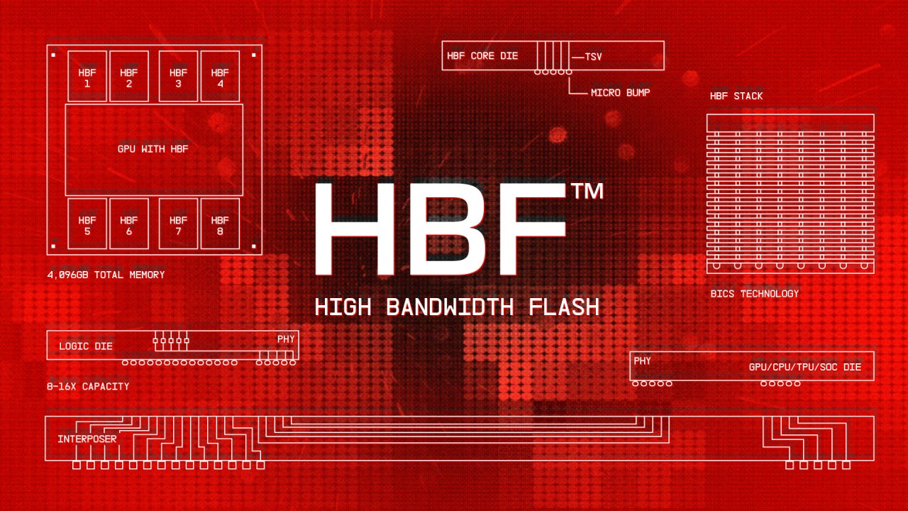
High Bandwidth Flash (HBF), jointly developed by SK Hynix and SanDisk, establishes a new memory tier strategically positioned between High Bandwidth Memory (HBM) and solid-state drives (SSDs). Leveraging advanced NAND stacking technologies—specifically 8-high and 16-high die configurations—HBF achieves capacities up to 512GB per stack with bandwidth scaling from 0.4 TB/s to 3.0 TB/s, rivaling HBM4’s 2.0 to 3.3 TB/s range. This balance of high capacity and competitive bandwidth is made possible through 3D packaging and TSV stacking techniques, enabling HBF to deliver HBM-like throughput while maintaining a footprint, power profile, and stack height compatible with existing HBM4 modules, facilitating seamless integration into AI accelerators such as GPUs and CPUs.
HBF’s technical role is to expand AI inference memory capacity and bandwidth by storing large volumes of read-intensive pretrained model weights closer to the GPU than traditional SSDs, thereby mitigating critical AI memory bottlenecks without displacing HBM. This tiered memory architecture positions HBM as the primary working memory for latency-sensitive and frequently updated data, while HBF serves as a high-capacity, read-optimized layer for inference workloads. Simulation modeling with Llama 3.1 demonstrated that systems using HBF achieved performance within 2.2% of configurations with unlimited HBM capacity, underscoring HBF’s effectiveness in maintaining near-HBM performance at significantly larger scales.
The adoption of the Universal Chiplet Interconnect Express (UCIe) standard in HBF’s design establishes an open, high-speed chiplet interconnect that facilitates flexible integration with diverse processors and accelerators, including GPUs and CPUs. This industry-backed specification encompasses comprehensive electrical, packaging, reliability, and software I/O guidelines, laying a robust foundation for HBF’s deployment as a scalable memory tier. By enabling massive parallelization of NAND flash areas—dividing over 5,000 memory layers in the largest configurations—HBF achieves high transfer rates that address the unique demands of AI workloads, balancing cost, capacity, and bandwidth in ways traditional memory hierarchies cannot.


Open Spec Reshapes AI Memory
HBF’s open, UCIe-based standard leverages mature NAND manufacturing to drive down costs and fuel scalable AI infrastructure, signaling a shift away from proprietary memory solutions and expensive HBM supply chains.
The High Bandwidth Flash (HBF) memory standard, jointly developed by SK Hynix and SanDisk with backing from AI giants like Google and Tenstorrent, emerges as a pivotal new tier positioned between HBM and SSDs to tackle AI inference memory bottlenecks. By offering up to 512GB capacity and bandwidth scaling from 0.4 to 3.0 TB/s, HBF addresses the growing demand for larger memory pools without the prohibitive costs of HBM, thereby expanding the memory capacity race critical for scaling AI workloads. This collaboration, highlighted at FMS 2026 and supported by an open specification through the Open Compute Project, signals a strategic industry shift toward more accessible, scalable memory solutions tailored for AI inference infrastructure.
HBF’s open specification, leveraging the Universal Chiplet Interconnect Express (UCIe) standard, is designed to foster a broad chiplet ecosystem that contrasts sharply with proprietary efforts from competitors like Samsung. This open approach not only encourages wider industry adoption but also integrates seamlessly with hybrid architectures such as SK Hynix’s H³, which unifies HBM and HBF on a single silicon interposer alongside GPUs. By enabling unified access to both high-bandwidth and high-capacity memory pools, this architectural innovation promises to significantly enhance AI inference throughput and efficiency, positioning HBF as a scalable, cost-effective complement rather than a replacement for HBM.
The strategic reliance on mature NAND flash manufacturing infrastructure for HBF production could reshape semiconductor supply chains by offering a more cost-effective and scalable alternative to capital-intensive HBM fabrication. This pragmatic use of existing high-volume NAND processes aligns with the AI industry's pressing need for affordable memory capacity expansion, especially as inference workloads prioritize memory size over extreme bandwidth. Consequently, HBF stands to become a key enabler in the AI memory hierarchy, balancing performance and economics to meet the surging demands of next-generation AI systems.